

The review “Revolutionizing Wearable Technology: Advanced Fabrication Techniques for Body‐Conformable Electronics” provides a comprehensive overview of the state‐of‐the‐art methods for fabricating flexible and stretchable electronic devices tailored for wearable applications. It discusses how traditional rigid electronics are giving way to innovative manufacturing processes that allow devices to seamlessly conform to the complex contours of the human body while maintaining excellent performance and reliability.
Overview of Wearable Electronics Challenges and Opportunities
The emergence of the Internet of Things (IoT) and artificial intelligence (AI) has spurred the need for electronics that are not only powerful but also mechanically flexible. Conventional fabrication methods cannot address the demands for lightweight, highly deformable, and durable devices. This review details how advanced fabrication techniques—ranging from printed electronics to 3D structure and deformation fabrication—have revolutionized the design and function of wearable devices. The integration of these techniques enhances design freedom, enables multifunctionality, and significantly improves the user experience in areas such as healthcare monitoring and human-machine interfaces (see Fig. 1 for an overview schematic).
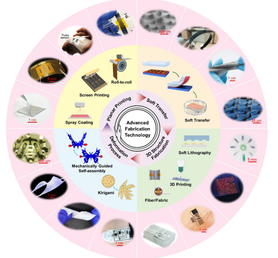
Fig 1
Printed Electronics Fabrication Technology
Printed electronics are at the forefront of wearable device production. Techniques such as screen printing, spray coating, and roll-to-roll (R2R) processing allow the deposition of conductive, semiconducting, or luminescent materials onto flexible substrates.
• Spray Coating: This method atomizes conductive inks (e.g., Ag nanowires, carbon nanotubes, MXene) and deposits them through stencils onto substrates. It is particularly effective for large-area coatings and has been applied to fabricate flexible OLED displays and sensor arrays (Figs. 2a–c).
• Screen Printing: Using a patterned screen as a stencil, this method delivers high-resolution patterns ideal for creating electrodes and circuit elements, as demonstrated by its application in fabricating electrodes for ECG monitoring (Figs. 2d–f).
• Roll-to-Roll Processing: R2R enables continuous, high-volume production by processing materials on a flexible roll. It has been successfully used for large-area devices such as perovskite solar cells, although it requires precise tension control and substrate compatibility (Figs. 2g–i).
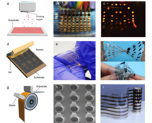
Fig 2a-i
Soft Transfer Technology
Soft transfer techniques are essential for moving delicate electronic structures from donor to receiver substrates. These methods focus on controlling adhesion and peeling forces to ensure efficient device transfer without damaging sensitive components.
• Thermal Release and Laser-Driven Non-Contact Transfers: In these methods, controlled heating (either via a thermal element or laser pulses) modulates adhesion forces to release devices onto new substrates. Laser-driven techniques allow for high selectivity, enabling the transfer of microchips below 100 μm.
• Shear-Assisted and Shape Memory Polymer (SMP) Transfers: By exploiting shear forces or the shape recovery properties of SMPs, these techniques facilitate the transfer of very small-scale devices with high accuracy.
• Surface Chemical and Adhesive Transfers: This method involves using an intermediate polymer layer and a sacrificial layer that is later etched away to leave the transferred device intact.
3D Structure Fabrication Technology
The need for complex three-dimensional architectures in wearable electronics has driven the development of several 3D fabrication techniques:
• Soft Lithography: This group of methods—including microcontact printing (μCP) and microtransfer molding (μTM)—enables the formation of micron- or nanoscale 3D structures on flexible substrates. They offer high-resolution patterning at low cost, though alignment and multilayer stacking can be challenging (Figs. 4a–d).
• Capillary Micromolding (MIMIC) and Solvent-Assisted Micromolding (SAMIM): These techniques rely on capillary forces and solvent-induced swelling, respectively, to accurately mold polymers into intricate 3D shapes.
• 3D Printing Methods: The review covers both photopolymerization techniques (stereolithography [SLA] and digital light processing [DLP]) and extrusion methods (fused deposition modeling [FDM], direct ink writing [DIW], and omnidirectional printing [ODP]). Photopolymerization offers exceptional resolution, whereas extrusion-based methods provide material versatility and scalability. These approaches have been applied to create flexible sensors, antennas, and even artificial skin.
Fiber/Fabric Technology
For applications in smart textiles and wearable fabrics, fiber-based techniques such as thermal drawing, electrospinning, and coating are key.
• Thermal Drawing: This process extrudes polymers at high temperatures to form fibers with controlled internal structures, useful for integrating conductive elements and even semiconductor wires.
• Electrospinning: Utilizing high-voltage fields, electrospinning produces nanofibers that can form nonwoven mats with adjustable surface roughness, ideal for sensor and drug delivery applications.
• Coating: Techniques that deposit functional layers onto fibers enhance properties like conductivity and durability. Automated coating methods have been developed for producing uniform MXene-coated yarns.
Deformation Fabrication Technology
To achieve extreme stretchability and adaptability, deformation-based techniques such as kirigami and mechanically guided assembly are employed.
• Kirigami Technology: Inspired by traditional paper-cutting, kirigami uses precise cutting and folding to convert 2D sheets into 3D structures. This approach enables the creation of devices that can withstand strains far beyond conventional materials, with applications ranging from wearable sensors to implantable devices.
• Mechanically Guided Assembly: By programming mechanical deformations through stress control or external stimuli, 2D structures are transformed into complex 3D architectures. This dynamic approach is suitable for applications such as flexible sensors and soft robotics, where real-time adaptability is crucial.
Conclusion
The article underscores that advanced fabrication technologies have not only addressed the limitations of rigid electronics but have also opened new avenues for innovation in wearable devices. By integrating printed electronics, soft transfers, 3D fabrication, fiber/fabric techniques, and deformation methods, manufacturers can now produce high-performance, body-conformable electronics. These technologies pave the way for next-generation wearable devices that are more adaptable, multifunctional, and seamlessly integrated into everyday life. The review’s detailed figures and schematics visually capture the progress and prospects of these fabrication methods, reinforcing the transformative impact on medical monitoring, human-machine interfaces, and IoT sensor networks.
This summary maintains the integrity of the original images and schematics, which are integral to understanding the complex fabrication processes discussed in the review.


